
 Home
Home


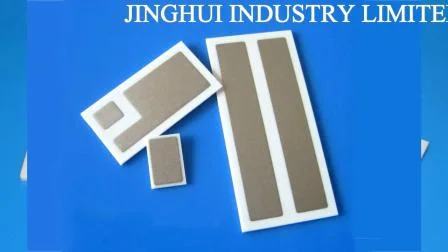
as Fired Aln Insulating Plate Bare Aluminum Nitride Substrate PCB
Basic Info.
| Model NO. | JJBP-0141-0013 |
| Usage | Blank Ceramic Circuit Board |
| Forming Method | Tape Casting |
| Transport Package | Individual Package |
| Specification | Max. up to 140mm× 190mm |
| Trademark | JingHui |
| Origin | China |
| HS Code | 8547100000 |
Product Description
As Fired AlN Insulating Plate Bare Aluminum Nitride Substrate PCBProduct Introduction
Aluminum nitride (AlN) is an advanced ceramic material for high power hybrid semiconductor packaging where high thermal conductivity is
required. AlN ceramic substrates have a thermal conductivity of more than 170W/m·K.
Molding Technique of the Aluminum Nitride Ceramic Substrate
Although dry pressing and isostatic pressing are suitable for producing high-performance aluminum nitride ceramic substrates, they are high in
cost and low in production efficiency, and cannot meet the increasing demand for aluminum nitride ceramic substrates in the electronics industry.
In order to solve this problem, in recent years, many manufacturers have adopted tape casting technique to produce aluminum nitride ceramic
substrates. Tape casting has also become the main molding technique for aluminum nitride ceramic substrates used in the electronics industry.
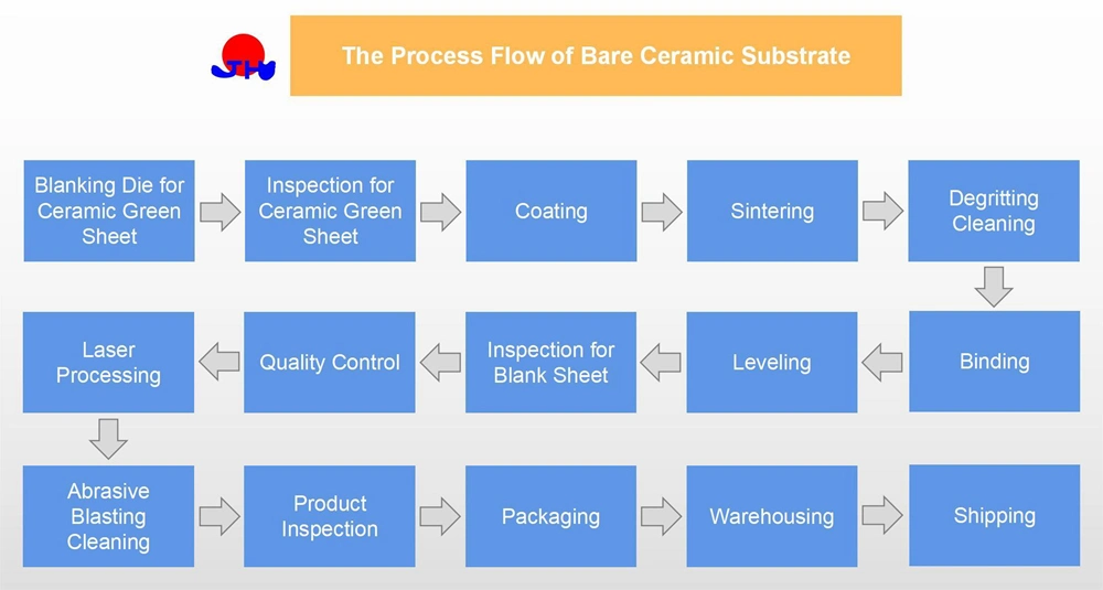
Manufacturing Capacity
The aluminum nitride ceramic substrate has high hardness and high brittleness, making it difficult to process. Most of the aluminum nitride ceramic
substrates are rectangular, square or round in shapes. Our rectangular shapes for as-fired aluminum nitride ceramic substrates are available up
to 140mm×190mm.
Below is the standard dimensions of our bare alumina substrates.
| AlN Ceramic Substrate | |||||||
| Thickness (mm) | Maximum Size (mm) | Shape | Molding Technique | ||||
| As-fired | Lapped | Polished | Rectangular | Square | Round | ||
| 0.1-0.2 | 50.8 | 50.8 | √ | √ | Tape Casting | ||
| ≥0.2 | 114.3 | 114.3 | √ | √ | Tape Casting | ||
| 0.38 | 140×190 | 140×190 | 120 | √ | √ | Tape Casting | |
| 0.5 | 140×190 | 140×190 | 120 | √ | √ | Tape Casting | |
| 0.635 | 140×190 | 200 | 200 | √ | √ | √ | Tape Casting |
| 1 | 140×190 | 300 | 200 | √ | √ | √ | Tape Casting |
| 1.5 | 300 | 200 | √ | √ | Tape Casting | ||
| 2 | 300 | 200 | √ | √ | Tape Casting | ||
| 2.5 | 300 | √ | √ | Tape Casting | |||
| 3 | 300 | √ | √ | Tape Casting | |||
| … | 450 | √ | √ | Isostatic Pressing | |||
| 10 | 450 | √ | √ | Isostatic Pressing | |||
| Other special thicknesses within the thickness range of 0.1-3.0mm can be achieved by lapping. | |||||||
For material properties, please refer to the table below.
| AlN Ceramic Substrate | ||
| Item | Unit | Value |
| Mechanical Properties | ||
| Color | / | Gray |
| Density | g/cm³ | ≥3.33 |
| Flexural Strength | MPa | ≥380 |
| Water Absorption | % | 0 |
| Camber | Length‰ | ≤3‰ |
| Thermal Properties | ||
| Max. Service Temperature (Non-loading) | ºC | >1000 |
| CTE (Coefficient of Thermal Expansion) | 20-800ºC, 1×10⁻⁶/ºC | 4-6 |
| Thermal Conductivity | 20ºC, W/m·K | 170-230 |
| Electrical Properties | ||
| Dielectric Constant | 1MHz | 8-10 |
| Volume Resistivity | 20ºC, Ω·cm | ≥1013 |
| Dielectric Strength | KV/mm | ≥17 |
Q1: What is the Maximum Service Temperature of the Aluminum Nitride Ceramic Substrates?
Aluminum nitride ceramic substrates can withstand high temperature over 1000 ºC.
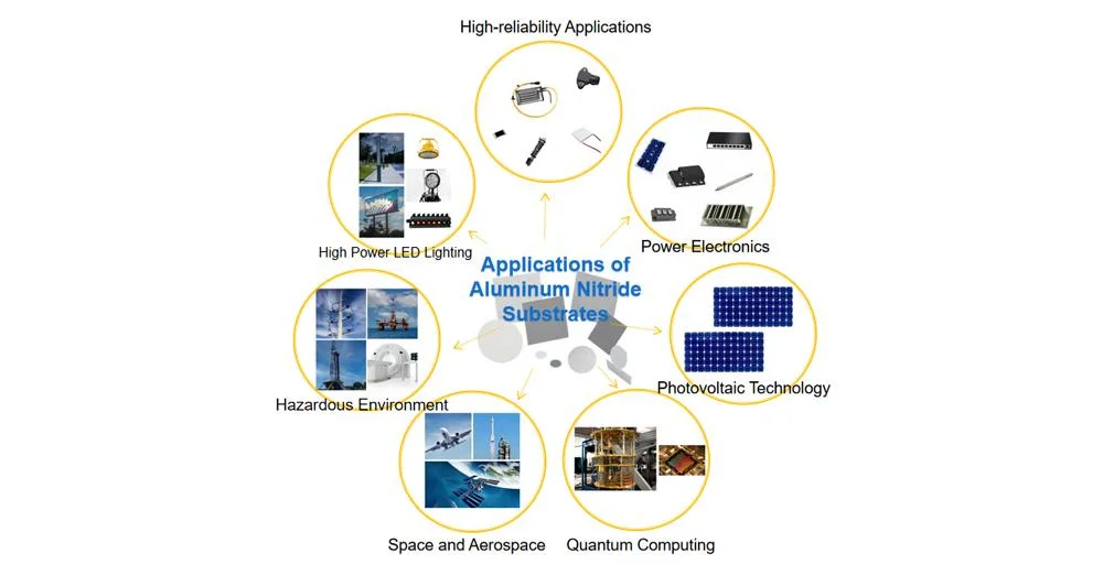
Q2: Do the Bare Ceramic Substrates Meet the Requirements for Metallized Ceramic Circuit Boards?
Yes. Metallized ceramic substrates, also known as metallized ceramic circuit boards, include bare ceramic substrates and metal circuit layers. Bare
ceramic substrates are widely used in integrated circuit packaging, LED lighting, heat dissipation substrates and other fields in the electronic industry
due to their advantages of thinness, high temperature resistance, high electrical insulation performance, low dielectric loss, and good chemical
stability.
Q3: What is the Maximum Thermal Conductivity of Your Bare Aluminum Nitride Substrates?
The thermal conductivity of aluminum nitride substrates is generally 170W/m·K or higher. The maximum value can reach 230W/m·K, which is 8 times
that of alumina. It has broad development prospects in the fields like high-power electronic semiconductor modules, electronic heaters and
semiconductor power hybrid circuits.
Q4: Can We Get Free Samples?
Samples of standard sizes are free, and we only charge for shipping. If customization is required, we only collect sample fee for MOQ.
Q5: How Long is the Production Lead Time?
If the product is in stock, we will ship it within 1-2 days. The standard lead time for other orders is 4-6 weeks.
If your question is not listed here, please contact us for more information.